實驗室介紹影片
1. Catalyst-free synthesis of tungsten oxide nanowires via thermal evaporation for fast-response electrochromic devices
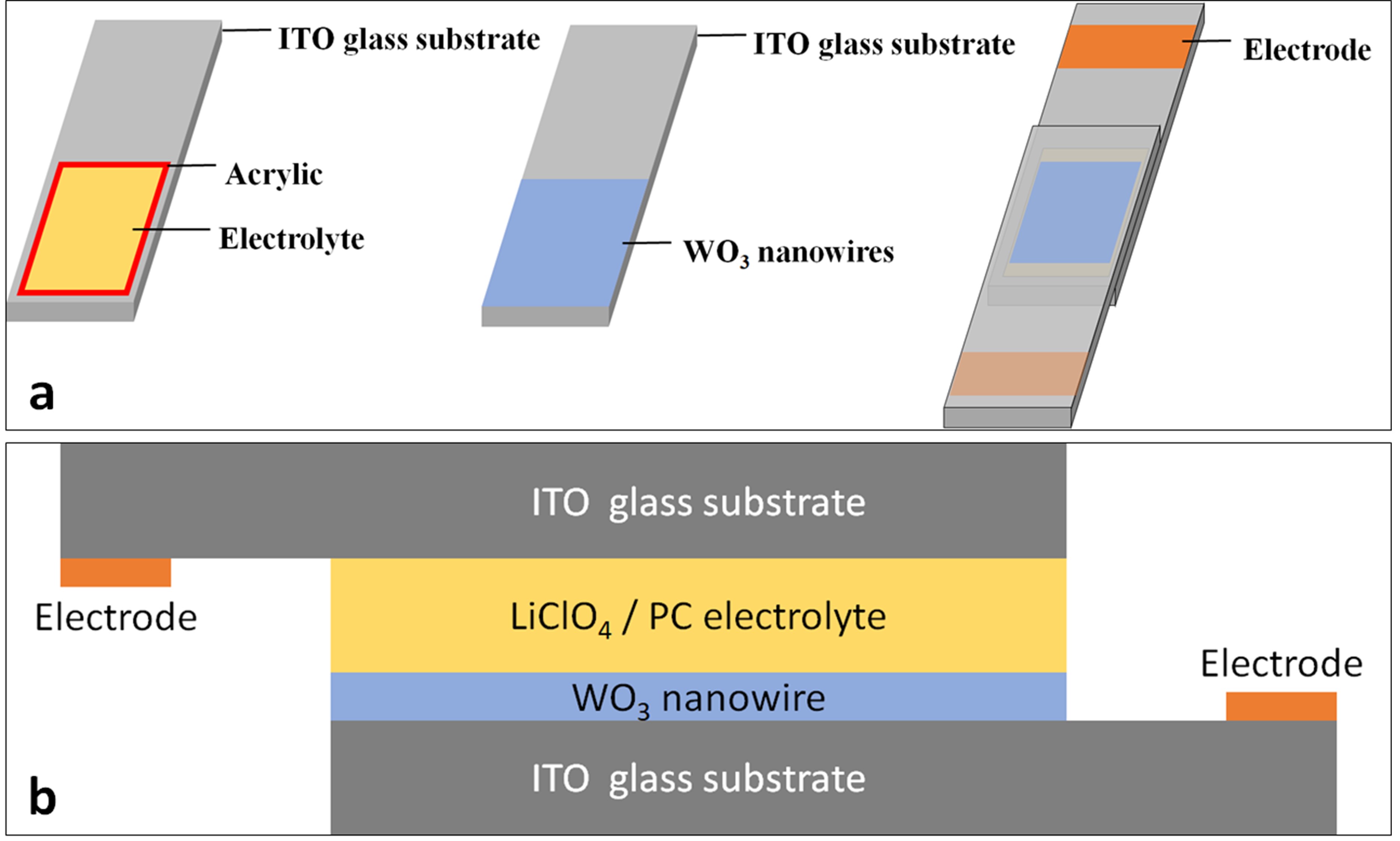
Tungsten oxide has drawn widespread attention due to its outstanding physical properties; however, the use of high temperature, low pressure, and expensive catalysts has been challenging in the synthesis of tungsten oxide nanowires. In this study, we developed a single step thermal evaporation process without any catalyst to synthesize WO3-x nanowires on silicon substrates and indium tin oxide glass substrate safely and economically. We utilized the Taguchi method to design experiments for the synthesis of tungsten oxide nanowires and analyze the effect of processing parameters. The growth mechanism of nanowires is proposed to be a vapor–solid mechanism. Confirmed to be oxygen-vacancy-rich WO3-x nanowires through high-resolution transmission electron microscopy studies, the nanowires have a great morphology with a high aspect ratio of around 700. The electrical resistivity of a single WO3-x nanowire at 300 K was measured to be 2.32 × 10⁻⁵ Ω M, which is relatively low due to rich oxygen vacancies. We synthesized WO3-x nanowires on an indium tin oxide glass substrate and assembled electrochromic devices with LiClO4/PC as the electrolyte. The devices were demonstrated to have fast coloring and bleaching rates of less than one second at low voltage; at high voltage, the color of the devices could change to a deeper color but take more than 2 seconds to react. Compared with previous works, the electrochromic devices from this study exhibit superior response time and stability. These significant results make WO3-x nanowires promising materials for applications in semiconductors, nanodevices, display and green technology.
CrystEngComm, Vol.24, No.47, 8213-8218 (2022)
2. Epitaxial growth and E-beam induced structural changes of single crystalline 2D antimonene
Two-dimensional antimonene has attracted much attention because of its excellent stability and remarkable physical properties. Understanding the growth mechanism of antimonene by investigating processing parameters and structural properties is necessary for developing reliable fabrication methods. In this study, NaCl-assisted van der Waals epitaxy, one of the methods for scale-up fabrication, is employed to achieve atomic layer antimonene with high coverage rate. Furthermore, high-resolution images of atomic structure are presented with the powerful transmission electron microscopy, helping us confirm the exact configuration of antimonene. Meanwhile, we studied the effect of electron beam irradiation on antimonene; it was found that the stacking structure of antimonene would change under electron beam irradiation, and the moire patterns of twisted few-layered antimonene were also observed. These results provide comprehensive study of growth mechanisms and in-depth knowledge of antimonene nanostructure, which are expected to facilitate the development of controllable fabrication for future device applications.

Scripta Materialia, Vol.226, No.6, 115262 (2023)
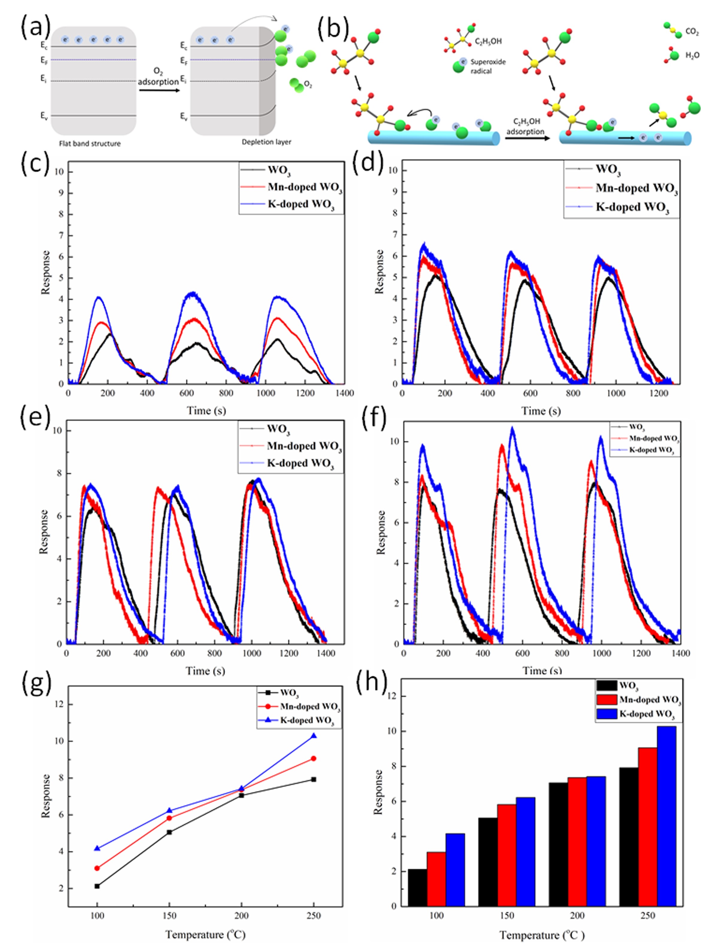
3. Chemical Vapor Deposition-Fabricated Manganese-Doped and Potassium-Doped Hexagonal Tungsten Trioxide Nanowires with Enhanced Gas Sensing and Photocatalytic Properties
Owing to its unique and variable lattice structure and stoichiometric ratio, tungsten oxide is suitable for material modification; for example, doping is expected to improve its catalytic properties. However, most of the doping experiments are conducted by hydrothermal or multi-step synthesis, which is not only time-consuming but also prone to solvent contamination, having little room for mass production. Here, without a catalyst, we report the formation of high-crystallinity manganese-doped and potassium-doped tungsten oxide nanowires through chemical vapor deposition (CVD) with interesting characterization, photocatalytic, and gas sensing properties. The structure and composition of the nanowires were characterized by transmission electron microscopy (TEM) and energy-dispersive spectroscopy (EDS), respectively, while the morphology and chemical valence were characterized by scanning electron microscopy (SEM) and X-ray photoelectron spectroscopy (XPS), respectively. Electrical measurements showed that the single nanowires doped with manganese and potassium had resistivities of 1.81 × 10⁻⁵ Ω·m and 1.93 × 10⁻⁵ Ω·m, respectively. The doping contributed to the phase transition from monoclinic to metastable hexagonal for the tungsten oxide nanowires, the structure of which is known for its hexagonal electron channels. The hexagonal structure provided efficient charge transfer and enhanced the catalytic efficiency of the tungsten oxide nanowires, resulting in a catalytic efficiency of 98.5% for the manganese-doped tungsten oxide nanowires and 97.73% for the potassium-doped tungsten oxide nanowires after four hours of degradation of methylene blue. Additionally, the gas sensing response for 20 ppm of ethanol showed a positive dependence of doping with the manganese-doped and potassium-doped responses being 14.4% and 29.7%, respectively, higher than the pure response at 250 °C. The manganese-doped and potassium-doped tungsten oxide nanowires are attractive candidates in gas sensing, photocatalytic, and energy storage applications, including water splitting, photochromism, and rechargeable batteries.
Nanomaterials, Vol.12, No.7, 1208 (2022)
4. Synthesis of morphology-improved single-crystalline iron silicide nanowires with enhanced physical characteristics
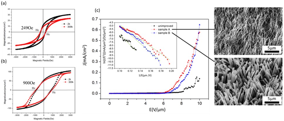
Single-crystalline iron silicide nanowires were synthesized via an original approach, pre-deposition method (PDM), with significantly improved morphologies and physical characteristics as compared with those fabricated by conventional chemical vapor deposition. In the pre-deposition method, combining rapid thermal annealing (RTA) and chemical vapor deposition (CVD), iron silicide nanowires grew from the heterogeneous nucleation sites on the surface of the thin film without a catalyst or Al2O3 template. The morphology of the nanowires has been considerably improved in terms of alignment and aspect ratio. HRTEM analysis confirms that the nanowires were β-FeSi2 with a crystal direction of [111]. Physical property measurements indicate that compared with CVD β-FeSi2 nanowires, β-FeSi2 nanowires synthesized by the PDM performed better in both the field emission and magnetic properties. Magnetic property measurements show that the coercive field of PDM nanowires increased from 249 Oe to 900 Oe. Field emission studies reveal that the average β value of the CVD β-FeSi2 nanowires was 1060, while that of the PDM nanowires became 1892. Notably, with a furnace, few researchers can successfully synthesize nanowires of β-FeSi2, which is one of the most fascinating silicides for its important applications.
CrystEngComm, Vol.23, No.18, 3270-3275 (2021)
5. Atomic Imaging of Molybdenum Oxide Nanowires with Unique and Complex Periodicity by Advanced Electron Microscopy
Crystalline Mo5O14 exhibits distinctive structural features such as tunnel structure and pseudolamellar arrangement according to the ideal model. However, the spatial resolution of the conventional technique of transmission electron microscopy (TEM) is insufficient to distinguish the actual positions of atoms. In this work, we aimed to systematically analyze and identify the Mo5O14 nanowires fabricated by the chemical vapor deposition (CVD) process. Utilizing high-angle annular dark-field (HAADF), annular bright-field (ABF), and enhanced annular bright-field (E-ABF) within the scanning transmission electron microscope (STEM) mode reveals the structural features at the atomic scale. In addition, the ultrahigh resolution images have confirmed the crystallographic insights in [001] growth direction for the Mo5O14 nanowires with a tunnel structure throughout the nanowire. The cross-sectional images show the unique close-packed plane and atomic arrangement with a network of MoO6 octahedra and MoO7 pentagonal bipyramids. These results are consistent with the theoretical atomic arrangement, supporting the realization of Mo5O14-type catalysts used in the selective oxidation process and battery applications.
Nano Letters, Vol.20, No.3, 1510-1516 (2020)
(Selected as a cover)
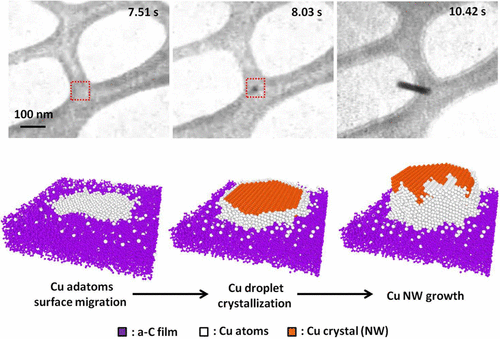
6. In situ Investigation of Defect-free Copper Nanowire Growth
The fabrication and placement of high purity nanometals, such as one-dimensional copper (Cu) nanowires, for interconnection in integrated devices have been among the most important technological developments in recent years. Structural stability and oxidation prevention have been the key issues, and the defect control in Cu nanowire growth has been found to be important. Here, we report the synthesis of defect-free single-crystalline Cu nanowires by controlling the surface-assisted heterogeneous nucleation of Cu atomic layering on the graphite-like loop of an amorphous carbon (a-C) lacey film surface. Without a metal-catalyst or induced defects, the high quality Cu nanowires formed with high aspect ratio and high growth rate of 578 nm/s. The dynamic study of the growth of heterogeneous nanowires was conducted in situ with a high-resolution transmission electron microscope. The study illuminates the new mechanism by heterogeneous nucleation control and laying the groundwork for better understanding of heterosurface-assisted nucleation of defect-free Cu nanowire on a-C lacey film.
Nano Letters, Vol.18, No.2, 778-784 (2018)
材料新館 44906室
Tel: +886-6-2365488